FPGA stands for Field Programmable Gate Array, which at first sight does not reveal too many details about what one of the most exciting forms of technology of the minute is. So, lets delve a little deeper.
Simply put, an FPGA is a unique kind of microchip. They are designed to be programmed at any time after installation into a system. The chips are programmed with a configuration which is the design of a complete digital logic circuit. FPGA engineers are able to generate configurations for circuits to perform all kinds of tasks. Just like the memory inside of a computer, FPGAs can be reprogrammed again and again with any circuit imaginable, limited only by the size of the device.
FPGAs are generic devices and can perform useful tasks in many situations. Here are some examples:
- Video processing
- Network switch
- Microprocessor emulation
- Image recognition
- Retro arcade machine
- High performance computing
Any type of digital processing that one would use a microchip for can be implemented in an FPGA.
Origins
The technology is by no means new, the first FPGA was developed by Xilinx in 1985. Early devices were small and could only contain simple circuits, however like all microchips their evolution has followed Moore’s Law. Rather than being able to be programmed with a few thousand logic gates, todays devices are able to be programmed with millions of gates. This has opened out the application of FPGAs to new and exciting spaces, such as finance.
Design
When an engineer develops for an FPGA, what they are doing is designing a circuit. A traditional computer program executes serially, however a circuit is multi-dimensional and able to perform sub-tasks in parallel with each other. This makes designing for FPGAs and a traditional computer a very different challenge. Although FPGA chips can be used for many tasks, once they have been programmed they are performing just one fully custom and tuned computing task, and they can be reprogrammed again and again.
Under the bonnet
How are FPGAs able to be configured to carry out different tasks? The chips themselves contain many small look up tables (sometimes called LUTs), which have just a handful of inputs and a single output. During configuration these look up tables are setup to perform exactly like a logic gate, with a truth table of inputs and outputs – you might remember truth tables and logic gates from school. An FPGA can contain millions of look up tables – a so called “sea of gates”. In a today’s FPGAs memories and high performance I/O drivers augment the sea of gates. Finally configurable switches allow all these elements to be connected to each other in any fashion.
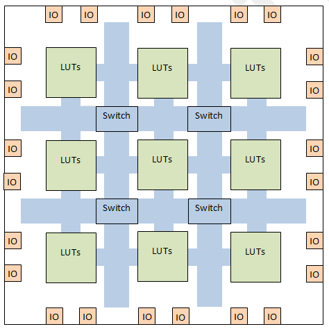
Under the bonnet of an FPGA
The FPGA compilation tools “synthesise” what the setup of all of the elements inside the FPGA need to be to perform in the same way as the designer’s circuit. This synthesis process can take minutes to hours.
FPGA?
So to finish this article, we now have all the information to explain what “FPGA” means. They are Field Programmable, because they can be reprogrammed at will in the field, inside a system. Inside the devices themselves they have a Gate Array – many small tables which can be configured and connected in any fashion as a digital circuit.
The larger FPGAs available today can carry out alot of compute very quickly, and are suited to many exciting tasks, though this blog will focus mainly on the financial space.
