Coding for FPGAs

In a slight change from my previous plans, I want to talk about different ways of programming FPGAs.

This can often be a fiercely controversial subject, with many advocates of the different methods. But I don’t believe the subjects needs to be controversial. To begin with, lets overview the process of building some FPGA code:

if this has been used, it typically compiles the following, or most people still code at this level directly:

tools provided by the FPGA manufacturers then allow:

  • Mapping – breaks down the design into resource elements present on the FPGA
  • Place and Route – places those elements on an FPGA, and determines routing
  • Timing check – ensure the design meets certain performance criteria
  • Bit stream generation – makes the actual FPGA programming file

The Place and Route/Timing check steps often occur iteratively. If timing checks fail, a different placement attempt is made.

Register Transfer Level

To a certain extent, these last steps are outside of a designers hands, algorithms provided by FPGA manufactures are used for all the steps – these algorithms can be guided, but they work with heuristic techniques such as simulated annealing.

FPGA designers have the biggest input with their code, which is usually at the Register Transfer Level (or RTL – to be explained shortly) or perhaps at a higher level.

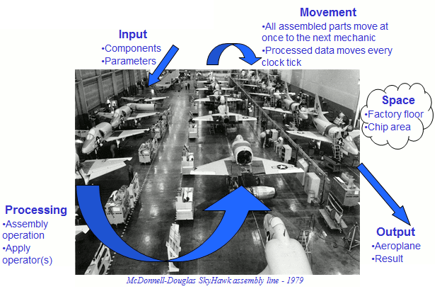
What is meant by a RTL language is that the designer specifies the changes in the states of the internal connections of the design between clock ticks. We talked about clock ticks in a previous blog entry, but an internal connection in this case means just that – a single wire with in the FPGA – whether it changes to a 1 or 0.

This is incredibly low level, RTL languages do provide some abstractions for buses (collections of wires), and the ability to modularise code and simulate, but essentially it deals with the states of individual wires.

Today, the RTL approach is the one used for most designs, even the complicated designs used in financial applications. The two main languages are VHDL and Verilog. In terms of features, these languages offer pretty much the same thing, though the syntax is different.

Needless to say, controversy exists as to whether VHDL or Verilog is the best approach to use. In my own opinion, since they offer more or less the same tools to a designer, I prefer them equally. Any reasonably experienced FPGA designer should be able to switch between both approaches in any case.

Not used so often today, but still possible, is schematic capture where a CAD tool is used to draw a circuit diagram by hand. Essentially, its equivalent to an RTL.

RTL languages give a high level of control to a designer, making low level optimisations possible, and allowing precising timing of certain operations.

Higher level languages

However the problem with RTL is that the programming is a such a low level that things taken for granted by software programmers are not possible. For example, changing the number system of part of a calculation.

Since the way to carry out arithmetic operations changes depending on the number system used, changing the number system leads to large and painful re-writes of code when it is done.

There are a number of varied alternatives for higher level FPGA programming languages, however at this time, despite a number of initiatives and much hype, no genuine standards have been widely adopted by the industry.

Higher level languages have been tarnished with a bad reputation – often ambitious marketeers have promised these languages as a silver bullet to reskilling software programmers into hardware designers. This is clearly not the case and will never be in all likelihood. The paradigm between programming CPUs and FPGAs is too different. The resources, optimisation methods, design granularity etc are all worlds apart. The two need a different mentality and no tool will change that.

Nevertheless, I do believe a higher level approach has much to offer the FPGA designer in terms of their efficiency as engineers, can help alot to reduce design times, and generally make our lives easier.

Types of higher level language

As I’ve indicated, a number of higher level approaches to FPGA design have been proposed. Due to the conservative nature of the space, these have seldom had an impact.

Generally the approaches fit somewhere between being a fully featured language (Impulse C, Handel C) and very narrow domain specific tools. Somewhere in between sit the so called “stream compilers” (or example OpenCL). I’ve worked with and designed a few of these myself, and they are all equally valid approaches depending on the aim of the designer.

Luckily, no one has to be restricted into using a single approach, compiler or language on a design. Its possible to mix and match. In my opinion the best approach is to use an RTL where its really needed, for designing interfaces etc. Domain specific compilers can then be used for the computing blocks – taking the hard work out of defining number systems/data types, and rebalancing pipeline branches to the same length.

Also, by performing simulations and debugging at a high level, its possible to turn around changes much more quickly, than going through a full compilation cycle.

As the name domain specific compiler suggests, its rarely possible to use one for a whole design. There is so much hype and misinformation in this space, it is hard for the inexperienced to say whether one high level tool or another is appropriate for a particular purpose.

Ambitious

Since no standards are really defined in the space of high level compilers, I would even encourage designers to make their own. Scripting languages easily allow the mapping of a high level pipeline description into VHDL, and you can save yourself alot of time this way. It will be a tool you understand and can develop in the direction you need it.

Advertisement
Posted in Uncategorized | Tagged , , , , , , | Leave a comment

FPGA vs CPUs ii

Last time I pointed out that although a number of applications run faster on FPGAs, not all of them do. This time I’ll be looking at which characteristics allow certain applications to run faster on FPGAs than CPUs.

To do this we first need to understand some of the principals of optimising designs on an FPGA. The standard design concept on an FPGA is the same as that used to design any other synchronous logic circuit: pipelining. To get the best performance from an FPGA designers usually aim to make their design what’s called “fully pipelined”. A fully pipelined design allows each component of the system to provide calculation towards the output at once, making it highly efficient.

Pipelining

Pipelining’s approach is similar to a factory assembly line, with the processing broken down into sections. Each section of processing is connected together in series, with the output of one section connected to the input of the next. Data moves between each section of
processing synchronously at regular intervals. Although each section of processing is conducted serially on an individual datum, the processing elements are all running in parallel, processing new data as it enters the system. Have a look at the image below of a
fighter jet assembly line to see what I mean:

Image

Raw materials, data, enter the assembly line. Each stage of assembly may be seen as a stage of a calculation, with data being combined together using operators. The output of the assembly line, the finished planes, would be the same as the result of the calculation in
this metaphor. The clock rate of a pipeline refers to the speed at which parts move from one assembly stage to the next. For the pipeline to work without buffering parts/data, this rate should be the same for every pipeline stage.

Pipelining in itself doesn’t decrease processing time, it could increase it. However pipelining will increase the throughput of a system when processing a stream of data. In terms of processing network data, a pipeline clocked at the same rate as incoming traffic can guarantee to process each byte of network data, even at 100% utilisation.

For example, in a 100 stage 1G network processing pipeline, clocked at 125MHz, the first byte of network data is processed in 800ns, with each subsequent processed byte arriving every 8ns. This is the same rate as data enters the system, irrespective of network
utilisation.

A CPU uses a pipeline for its processing too, and usually they run at a much faster rate than one on an FPGA. However, the pipeline on a CPU is not being used to its full capacity – not all stages are being used at once. It is as if on the production line some staff are having a coffee break. So CPU pipelines are not operating at peak efficiency. This is why optimised FPGA designs are able to run certain types of calculations faster than CPUs, despite a lower clock rate, since the pipeline can be designed so that each stage is always being used.

To come back to the original premise for this entry – which characteristics allow certain applications to run faster on FPGAs than CPUs? As you may be able to recognise by now, applications which can be mapped into a fully pipelined FPGA implementation, or a near fully pipelined implementation work the best.

Some points to think about to achieve full pipelining:

  • Do similar operations need to be carried out on each piece of data?
  • As few changes to pipeline behaviour with external state as possible
    • In the factory metaphor, this would be minimising the number of optional extras so that there are minimal branches in the assembly line/pipeline. In other words it’s best to have the data flow completely serial.
  • Accesses to external and internal resources. such as memory should be pipelineable, so that they can be integrated into the assembly process.
  • Parts of the algorithm may have to be refactored to pipeline them. Is this possible?
  • Does data arrive at a constant rate?
  • Accuracy – can precision be sacrificed to improve the rate moving data between stages of the pipeline?

Some applications in the financial space which can be pipelined to work well on FPGAs are Monte Carlo simulation and network processing.

Hard numbers

Next time I’ll most likely go into detail with case studies, but I promised hard numbers this time so to finish up with some.

“FPGA accelerated low-latency market data feed processing” was a research paper I co-wrote with David Thomas and Wayne Luk of Imperial College. It showed an FPGA based parser for the high-bandwidth OPRA feed was able to process all data on the feed up until the point of Ethernet saturation with no dropping of packets caused by slow processing. However, the software consuming the data delivered by the FPGA began to drop packets at around half line rate due to not being able to process the market data at the same rate.

An investigation into implementations of a European option pricing benchmark I conducted with Matt Aubury (“Design Space Exploration Of The European Option Benchmark Using Hyperstreams”) compares FPGA with alternative implementations including a software one using a conventional CPU. Depending on the accuracy criteria of the benchmark, the FPGA was shown to be between 15 to 146 times faster than the software implementation.

The numbers don’t lie – see you next time!

Posted in Uncategorized | Tagged , , , | Leave a comment

FPGA vs CPUs (or why bother with FPGA)

Before diving into some deeper technical content, I thought it would probably be a good idea to talk about why people in the finance sector are becoming interested in FPGA technology. I’ve personally been involved with FPGA projects in the world of finance since 2006, so this technology is something people have been sniffing around for quite a while. But the view of the industry in 2013 generally seems to be that this is something that will become a little more mainstream this year.

Clearly, this interest wouldn’t occur if people didn’t percieve a benefit over the status quo, but what are those benefits and are they real?

State of the art technology today, and for many years has been data centres full of commodity servers built around an Intel or Intel derived processor or CPU. These servers won’t suddenly be disappearing of course! These general purpose servers are designed for performing a wide variety of different tasks, using the same digital circuit on the silicon of the processor.

Multicore CPUs today can have tens of individual processors per device, each able to run a number of different tasks independently, and switch between them within a few microseconds. The processors also have access to large amounts of memory. It’s a decent solution to alot of compute problems.

CPUs gain their flexibility by being based around a fixed yet versatile architecture, however this architecture is not always used efficiently to address a problem. As we’ve already seen, FPGAs have a different approach. As any digital circuit can be implemented this allows a fully custom architecture to address a specific problem in the most efficient way.

It doesn’t take too much imagination to realise that if compute happens faster, in finance trades can occur faster, leading to greater profitability.

But, there are disadvantages to FPGAs. Although FPGAs can be reprogrammed, they can just ‘be’ one circuit at any one time, the reprogramming procedure takes several seconds. Also, the programming concept is different. With a CPU a program is a list of steps carrying out operations on data, where as an FPGA is programmed with a circuit. With traditional FPGA programming methods, this makes development effort much higher for FPGAs than CPUs. New, faster, FPGA development approaches are likely to be the subject of a future blog.

The different architecture and programming methodology means not all computing tasks can be implemented on FPGAs in a more efficient way than a CPU. However, there are many places where FPGAs can help. Examples of applications where FPGAs can offer acceleration in the financial domain include:

  • Monte Carlo pricing algorithms
  • Network processing
    • Market data feed handling
    • Compression (eg in a wireless link)

Next time, I’ll be continuing this look at FPGA vs CPUs. I’ll discuss what features make an application likely to run faster on FPGAs than CPUs. I’ll also be discussing some hard numbers for this, derived from some of my academic work. Tune in!

Posted in Uncategorized | Tagged , , , , , , | 1 Comment

What are FPGAs?

To provide some immediate background for people new to the technology, I’ve created a page “What are FPGAs?” which can be accessed on the top bar.

Posted in Uncategorized | Tagged , , , , | Leave a comment

Welcome

Welcome to this blog which will collect together various ideas about the use of FPGA technology in the world of finance. Content will include high level philosophical issues, as well as low level design techniques.

I’ve already collected a number of ideas for articles, and look forward to sharing them with you all in the coming months. Please don’t hesitate to get in touch if theres anything you’d like to see covered!

My work in the field of FPGAs has been continuing for over 14 years now, and more than half that has been in finance. I’ll be drawing not only on this experience in my posts, but also some relevant points from my doctoral research. Enjoy!

Posted in Uncategorized | Tagged , , , , | Leave a comment